
Go to the HOMEPAGE of this site, so that you can navigate through it, and find my e-mail address.
If your browser does NOT support FRAMES (The current page does not have them, but others do), please click HERE . You will arrive at the HOMEPAGE of this site (without FRAMES). From there you can navigate through this website by means of the links in the CONTENTS-section.
                                               back to Part One
                                               to bottom
This instruction (statement) means : Take the value of variable X and add it to the value of the variable Y. Assign the resulting value to the variable Z.
This instruction can be entered from the computer's keyboard. But the computer can execute it only when it is translated into machine-code. Let us see how things go, using the above PASCAL-statement as an example :
PASCAL-statement :
Z := X + Y;
This will first of all be translated into Assembly Language, which anatomizes the statement in several more basic statements such as:
COPY AX,X [ = get the quantity called X ]
ADD AX,Y [ = get Y and add it to the first quantity ]
COPY CN1,AX [ = store the result ]
COPY AX,CN1 [ = take the result ]
COPY Z,AX [ = put it into Z ]
This must now be translated into Machine Language Code, such as :
00101101
01101010
--------
--------
The Codes 00101101, 01101010, ... will be executed by Electric Circuitry.
In a computer there are two types of circuit,
The Instruction Register holds an (machine-code) instruction, like 00101101, telling what to do. Then the Code Deciphering Circuit deciphers the code and activates one of the Operation Circuits which will do the work, such as an arithmetic operation, on data which are stored in data registers, called X1, X2, ....
Operation Circuits
[ See BIERMANN, 1990, Great Ideas in Computer Science ].
In order to explain the workings of all these circuits, we must start with very simple circuits and gradually end up with real computational and storage circuits.
We begin with computational (operational) circuits. Such circuits can compute Boolean functions. These are functions with variables having two values only, which can be symbolized with (value) 0 and (value) 1. So a Boolean variable named X can assume only two values, 0 or 1. The values of such Boolean variables can serve as INPUT for a specified BOOLEAN FUNCTION, and result in a definite OUTPUT. Since each input results in only one output, we indeed have to do with a FUNCTION, the output is unambiguously determined by the input. Normally the input of a Boolean function consists of a configuration of values of several variables, say, X1, X2 and X3. Given each relevant input (configuration), the assignment of their proper outputs means the computation of that function.
A simple Boolean function could be the following :
X1    X2    X3        f(X1,X2,X3)

0     0     0        0
0     0     1        0
0     1     0        1
0     1     1        0
1     0     0        1
1     0     1        1
1     1     0        1
1     1     1        0
This function is said to be computed if and when :
0 is attributed to [000] 0 is attributed to [001] 1 is attributed to [010] 0 is attributed to [011] 1 is attributed to [100] 1 is attributed to [101] 1 is attributed to [110] 0 is attributed to [111]
It is the Operation Circuits that should compute such functions.
We now present a very simple Boolean function :
X      f(X)

0      0
1      1

We can express this function as f(X) = X (the Identical Function)
This function can be physically executed by a simple electric circuit, that allows to be in two states :
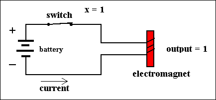
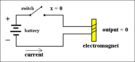
Figure 1. Two states of a simple circuit, computing f(X) = X. Each state represents a value of the variable X.
In the figures we must conceive of the switch being pulled in order to close it. We interpret (the switch) PULLED DOWN as the value of X being 1, and (we interpret) NOT PULLED DOWN as the value of X being 0.
In this particular circuit PULLING DOWN the switch results in the CLOSURE of that switch, and NOT PULLING DOWN the switch results in the OPENING of the switch, because we stipulate that the switch is made of spring material, resulting in its bouncing back to its OPEN position if not pulled (down) on.
In all circuits and with respect to all the types of switches we always interpret PULLING DOWN as the value of the associated variable being 1, and NOT PULLING DOWN as the value of the associated variable being 0 The action of PULLING DOWN is imagined to be performed by an electromagnet. This magnet, when it is on, will subject the switch to a pull. This magnet, together with its associated switch, is called a relay. Relays played an important role in the first electric digital computers.
A second switch type is the NOT-switch. When the value of the associated variable in such a switch is 1, i.e. when the switch is subjected to PULLING DOWN, it will OPEN. When the value of that variable is 0, i.e. when the switch is NOT subjected to PULLING DOWN, it will CLOSE. Also here we will imagine the switch being made of spring material, so when it is not pulled down it bounces back to its CLOSED position.
A not-switch embodies the following function :
X      f(X)

0      1
1      0

We can express this function as f(X) = [NOT]X (the NOT Function)
This function can be physically executed by a simple electric circuit, containing the NOT-switch :
Figure 2. Two states of a simple circuit, computing the function f(X) = [NOT]X. Each state represents the value of the variable X. The circuit contains a NOT-switch.
Such a circuit we call a NOT-gate.
When we combine, say, two normal switches in a serial way in one and the same circuit, we get a circuit that can compute the AND-function :
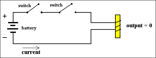
Figure 3. A Circuit that computes the AND-function. The first switch represents the variable X1, the second switch represents the variable X2. If the first switch is PULLED DOWN, X1 has the value 1. If the second switch is PULLED DOWN, X2 has the value 1. If the switches are left to themselves the variables have the value 0.
This AND-function (when we have it physically embodied by means of a circuit, then we can call it an AND-gate) gives output 1 if X1 and X2 have value 1. In the circuit this corresponds to both switches PULLED DOWN. We can write down the table of this AND-function as follows :
X1     X2      f(X1,X2)

0      0      0
0      1      0
1      0      0
1      1      1
This AND-function we can concisely formulate as f(X1,X2) = X1,X2, which means that its physical embodiment, i.e. the circuit that computes this function, consists of two (normal) switches wired serially. We can write down an AND-function with any number of variables, so let's take one with three of them :
X1    X2    X3        f(X1,X2,X3)

0     0     0        0
0     0     1        0
0     1     0        0
0     1     1        0
1     0     0        0
1     0     1        0
1     1     0        0
1     1     1        1
This is the function f(X1,X2,X3) = X1,X2,X3, implying a circuit with three (normal) switches wired serially :
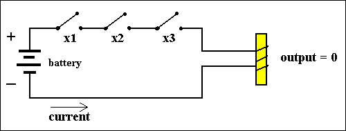
Figure 4. A circuit that computes the AND-function for three variables X1,X2 and X3. Only when all three variables have the value 1 the output of the function will be 1.
Aside from the Identical Function [ f(X) = X ], we have sofar treated of two elementary Boolean functions, the AND-function [f(X1,X2) = X1,X2 ] and the NOT-function [ f(X) = [not]X ].
A third elementary Boolean function is the OR-function :
X1     X2      f(X1,X2)

0      0      0
0      1      1
1      0      1
1      1      1
The output of this function is 1 if either X1, or X2, or both, have the value 1, otherwise it is 0. We can formulate this function as
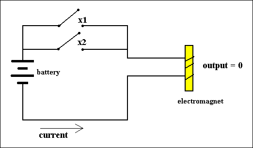
Fig 5. The circuit computing the OR-function. When at least one (of the two) switches is PULLED DOWN the circuit will output a 1. It will output a 0 otherwise.
This circuit we can call an OR-gate.
The three functions AND, NOT, and OR can be combined to compute any function of binary variables (when embodied in circuits). Thus with these elementary logical gates, AND, NOT, and OR, a universal computer can in principle be built, by allowing all kinds of combinations of them. Of course this can result in very complex circuitry.
Let us combine the AND and NOT function :
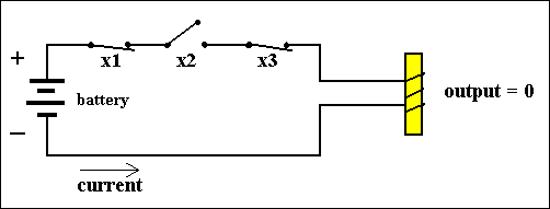
Figure 6. A combination of the AND- and NOT-gates.
The corresponding function-table is as follows :
X1    X2    X3        f(X1,X2,X3)

0     0     0        0
0     0     1        0
0     1     0        1
0     1     1        0
1     0     0        0
1     0     1        0
1     1     0        0
1     1     1        0
We can formulate this function as f(X1,X2,X3) = [NOT]X1 + X2 + [NOT]X3, expressing the fact that the circuit consists of three serially connected switches, of which the first switch is a NOT-switch, the second a normal switch, and the third a NOT-switch.
Another such combination of AND and NOT is the following Boolean function :
X1    X2    X3        f(X1,X2,X3)

0     0     0        0
0     0     1        0
0     1     0        0
0     1     1        0
1     0     0        0
1     0     1        1
1     1     0        0
1     1     1        0
The output of this function is 1 when X1 = 1 AND X2 = 0 AND X3 = 1, otherwise it is 0. We can formulate this function as f(X1,X2,X3) = X1 + [NOT]X2 + X3, meaning that the circuit consists of three serially wired switches, of which the first and third are normal switches, and the second a NOT-switch :
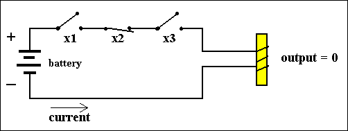
Figure 7. Another combination of NOT- and AND-gates.
The two functions, just expounded, can be combined in the " OR " combination :
X1    X2    X3        f(X1,X2,X3)

0     0     0        0
0     0     1        0
0     1     0        1
0     1     1        0
1     0     0        0
1     0     1        1
1     1     0        0
1     1     1        0
This is the function f(X1,X2,X3) = [NOT]X1 X2 [NOT]X3 + X1 [NOT]X2 X3, expressing the fact that the circuit consists of two parallel wired triplets of switches. The first triplet consists of a second switch which is normal, and the two other switches are NOT-switches. The second triplet consists of a second switch which is a NOT-switch, while the two other ones are normal switches :
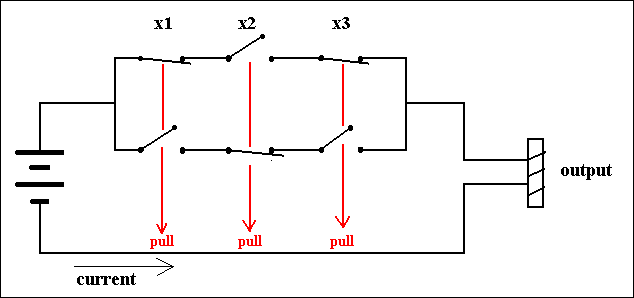
Figure 8. A Circuit that computes an OR-combination of two circuits. Switches, that are positioned above each other, are PULLED DOWN simultaneously (red arrows), expressing the fact that the corresponding variable has the value 1.
We imagine that each set of two (or more) above each other situated switches are PULLED down simultaneously by a controlling electromagnet (not shown in the figure). We see that the number of lines in the function-table that have 1 as output is two, and this means that the function shows two possible cases of outputing 1. This corresponds with the number of parallel series of switches in the circuit. So it is clear that we can set up a circuit for any number of 1's in the output of the function table.
Let us set up accordingly a circuit for the following function table which has again three variables, but now with three 1's in its output :
X1    X2    X3        f(X1,X2,X3)

0     0     0        0
0     0     1        0
0     1     0        1
0     1     1        0
1     0     0        0
1     0     1        1
1     1     0        0
1     1     1        1
This is the function f(X1,X2,X3) = [NOT]X1 X2 [NOT]X3 + X1 [NOT]X2 X3 + X1 X2 X3, expressing the fact that there are three parallel triplets of switches (with the two kinds of switches distributed as indicated) :
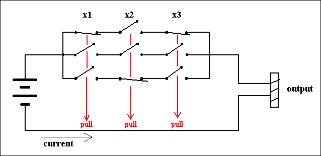
Figure 9. A circuit that computes an OR-combination of three circuits.
Relays
Our switches in the above expounded Operation Circuits are supposed to be operated electrically. They are pulled down by an electromagnet as soon as such a magnet will come on, by letting an electrical current pass through its coil. Such a device, a switch-controlled-by-an-electromagnet is called a relay. So we stipulate that letting a variable X have the value 1 is equivalent to letting the current flow through the coil of the relay causing the associated switches to be pulled down. So relays are electrically operated switches by means of electromagnets. These switches were the basis for early computers and telephone systems in the first half of the twentieth century. During the 1940's and 1950's other electrically operated switches were used, namely vacuum tubes, and finally, since about the late 1950's, transistors are used, because of their reliability, small sizes and their low energy consumption.
In the exposition of basic computer circuitry on this website we shall not be concerned with vacuum tubes.
Let us visualize a circuit consisting of relays in the following figure. In this figure we see in fact five circuits, circuit 1 for variable X1, circuit 2 for variable X2, circuit 3 for variable X3, a circuit consisting of switches, and finally a circuit consisting of the coil of an electromagnet, which comes on when the output of the previous circuit is 1 (this electromagnet could become part of another relay). :
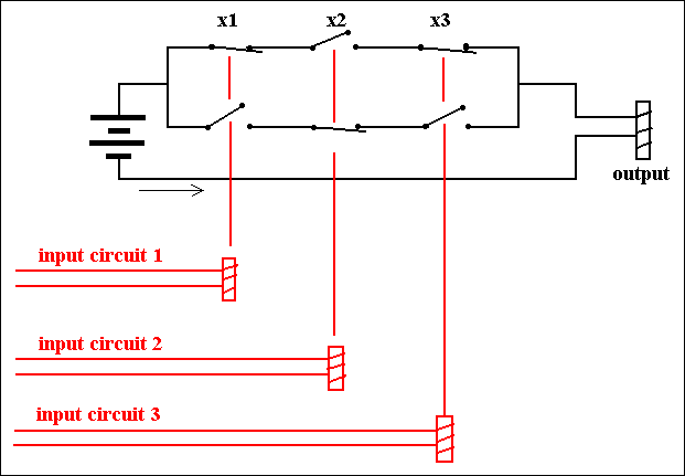
Figure 10. A circuit for a Boolean function and its associated electrical operation of the switches, by means of relays.
All this means that the techniques are complete and sufficient to compute arbitrarily complicated functions. We can write down the functional table for any target behavior with any number of binary input variables. The circuit that can compute that function can then be constructed with its electrical inputs and outputs. The inputs may be the results of other calculations, and the outputs may serve as inputs into many other circuits. Any individual circuit will act like a subroutine to the whole computation, and a large network of such circuits can perform huge tasks [BIERMANN, 1990].
Circuits for Storing Information
[ BIERMANN, 1990, Great Ideas in Computer Science ]
Whenever a complex computatation should be executed it must be possible to store information. This information to be stored can be data, or intermediary results of computations, which are necessary in later stages of the computation. When we feed an input in one of the above circuits, resulting in an output, then, when we switch off the input, the output will revert to its original value. So this output will not be retained.
We need circuits that will continue to give that same output, even when the input, which caused that output in the first place, is subsequently removed : The circuit must have memory. To construct such a circuit, we use the following idea :
In order to get an output value of 1, we must switch on an input-circuit (like the ones we see in figure 10), supplying an input-current, -- input 1. When we consequently switch off that input-current, then the output 1 still remains. But when we switch on another input-circuit, supplying another input-current -- input 0, the output will change to 0, and remains so, even when we switch off the current of input 0. So output can be produced, changed, and stored.
In order to understand how such circuits work, I will illustrate a circuit that can store one bit of information, that is, it can hold a 1 or a 0 (in order to know what it holds, only the answer to ONE question is needed, and this is what it means to hold ONE bit of information).
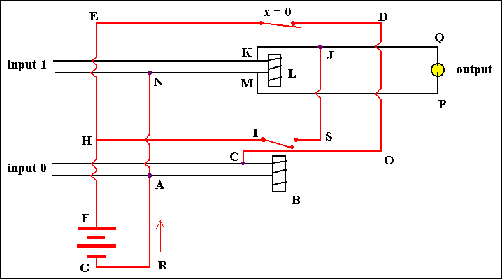
Figure 11. A Flip-Flop circuit to store one bit of information. Input 1 = off, input 0 = off.
With the aid of Figure 11. and the next figures we will explain the working of this one-bit storage circuit :
When both inputs (input 1 and input 0) are off the current will flow from G to R to A to B (the magnet comes on, and pulls the switch I down) to C to O to D to E (because the upper switch is closed, i.e. NOT PULLED DOWN, implying X = 0) and then back to the positive end of the battery (F). The output is 0, because input 1 is off, and because the flow from the battery can, it is true, pass through the output device (we can imagine it to be a light bulb), but cannot flow back to the battery : it ' tries ' to flow from G to R to A to N to M to P to Q to J to S, but is then blocked, because the switch I is open.
So we have : input 1 is off, input 0 is off, implying X = 0 and output = 0.
Now we look at the next figure :
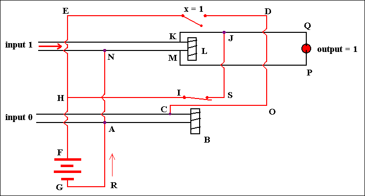
Figure 12. A Flip-Flop circuit to store one bit of information. Input 1 = on, input 0 = off
We now put input 1 on (figure 12.). Because of this the upper magnet comes on and PULLS DOWN the switch, which means that X = 1. But now the current going from G to R to A to B to C to O to D will be interrupted because of the open upper switch. So it cannot return to the positive end of the battery, and this causes the lower magnet (B) to become off implying the lower switch (I) to close. This means that the lamp (the output device) is fed by two currents. One from input 1, and the other from the battery : From G to R to A to N to M to P through the lamp tp Q to J to S to H (because the switch I is closed) to the positive end of the battery (F). Also the upper magnet is on because of those two currents.
So it is clear that when we shut down input 1, the upper switch remains PULLED DOWN, implying X = 1, and the lamp remains on (output remains 1). The next figure illustrates this situation.
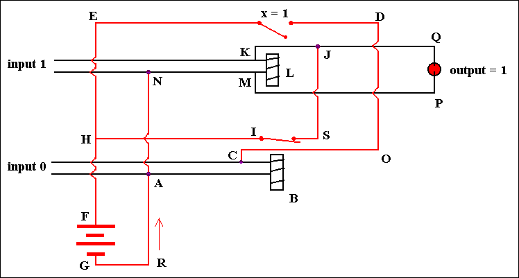
Figure 13. A Flip-Flop circuit to store one bit of information. Input 1 = off, input 0 = off
We now switch input 0 on. We will then obtain the situation as seen in the next figure :
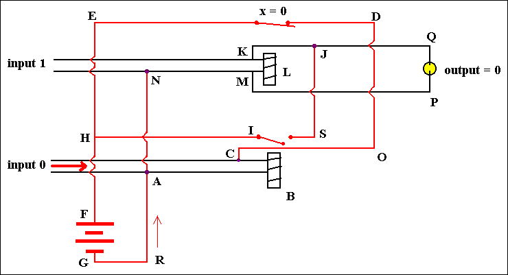
Figure 14. A Flip-Flop circuit to store one bit of information. Input 1 = off, input 0 = on
So when we switch input 0 on, then the lower magnet will come on and the switch I will be opened. This implies that the lamp does not receive current anymore (output becomes 0) because the current, flowing from G to R to A to N to M to P to Q to J is blocked just after S, because the switch I is open. For the same reason the upper magnet will go off, implying the upper switch to be closed. This implies that the lower magnet receives two currents, one from input 0, and one from the battery : From G to R to A to B to C to O to D to E and back to the positive end of the battery (F). Because the upper switch is closed, i.e. NOT PULLED DOWN, X = 0.
So we have : Input 0 = on, input 1 = off, implying X = 0, and output = 0.
Let us now shut down input 0. In this case the lower magnet still receives current, so the switch I remains open. This implies that there still cannot pass current to the lamp (the output remains 0), because current from G flowing to R to A to N to M to P to Q to J is blocked just after S. For the same reason the upper magnet remains closed, i.e. NOT PULLED DOWN, implying X = 0. So the original situation (Figure 11) has reappered.
We now have described a circuit that can store one bit of information. Such a circuit is called a Flip-Flop. And, now we know the workings of it, we can picture it (much more) schematically as follows :
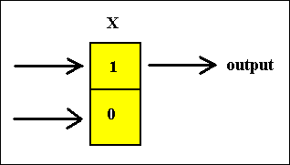
Figure 15. A Flip-Flop, able to store one bit of information. When input 1 is switched on the Flip-Flop will store a 1 as the value of the variable X. When input 0 is switched on the Flip-Flop will store a 0 as the value of the variable X.
In most commercial computers, information is stored in registers that are often made up of, say, 16 or 32 such Flip-Flops (they are thus called 16-bit or 32-bit registers, respectively). Now we can code information into strings of 0's and 1's and these strings can be stored in (a corresponding series of) Flip-Flops. So for example the number 18 can be expressed in eight binary digits as 0 0 0 1 0 0 1 0 and can be loaded into an 8-bit register as can be seen in the next figure.
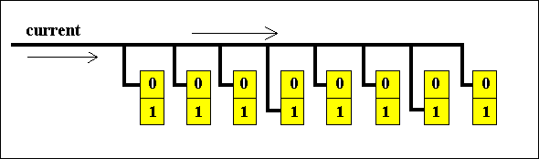
Figure 16. An 8-bits register storing the number 18
0 + 1 = 1, carry = 0

  01101
  01110
+ -----
      1

Again, 1 + 0 = 1, carry = 0

  01101
  01110
+ -----
     11

1 + 1 = 0, carry = 1

   1
  01101
  01110
+ -----
    011

1 + 1 + 1 = 1, carry = 1

  11
  01101
  01110
+ -----
   1011

0 + 0 + 1 = 1, carry = 0

  11
  01101
  01110
+ -----
  11011
This number 11011 has the value 24 + 23 + 21 + 20 (= 1) = 27. Indeed we have done the calculation 13 + 14 = 27.
Addition is a column-by-column operation, so we begin by examining a single column (BIERMANN, 1990, pp. 199). See Figure 17. The top register Xc in the column will hold the carry from an earlier calculation. The second and third registers X1 and X2 will hold digits to be added. The lowest register Xs will hold the sum of the column addition, and the carry will be transmitted to the next column to the left.
Besides the registers (which are themselves circuits -- storage circuits) we need two more circuits, one called Fs to compute the binary sum digit, and the carry circuit Fc to compute the carry digit. The input to these functions are Xc, X1, X2, and a variable called Xa, which is 1 if the addition is to be performed, and 0 otherwise, i.e. Xa serves as a switch to turn the adder off and on.
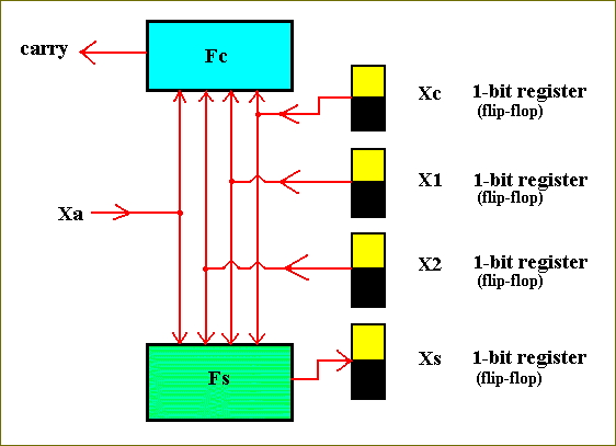
Figure 17. A single digit adder.
Given (1) the case that the adder can be switched on, and (2) knowing how to add binary numbers, we can now construct the table for these functions :
Xc    X1     X2    Xa          Fs    Fc
---------------------------------------
*     *      *     0           0     0
0     0      0     1           0     0
0     0      1     1           1     0
0     1      0     1           1     0
0     1      1     1           0     1
1     0      0     1           1     0
1     0      1     1           0     1
1     1      0     1           0     1
1     1      1     1           1     1
---------------------------------------
In this function table, defining the two functions Fc and Fs, Xc is the variable containing the value of the carry from an earlier calculation. The values of Fc are the newly computed carries. The values of Fs are the sums of the digits. The asterisk * stands for any input. If Xa = 0, i.e. if the adder-circuit is turned off, then, with whatever inputs of Xc, X1, and X2, the values of Fc and Fs will be 0.
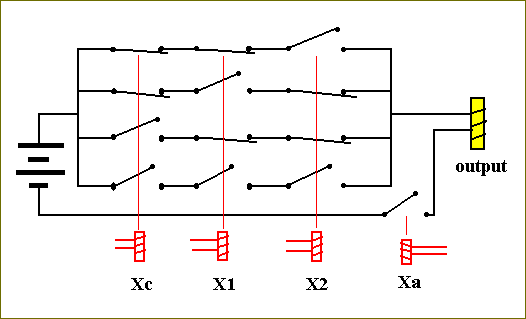
Figure 18. The circuit for computing Fs.
In the same way we can construct the carry-function Fc :
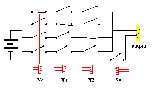
Figure 19. The circuit for computing Fc.
A third circuit is necessary. It is the circuit that activates Xa. If and when Xa is activated, i.e. when Xa = 1, then the ADD-circuit will be turned on (The ADD-circuit consists of the circuit for Fc and the circuit for Fs). This third circuit computes the Recognize-function. Before I give this circuit, let me explain its role. In a typical computer, there may be many instructions to operate on registers X1 and X2, for example instructions to multiply, divide, subtract, move etc. The addition-circuitry is only a small part of the whole architecture, and there must be provided means to turn it on when it is needed and to leave it inactive otherwise. This controlling can be done by means of an instruction-register. An operation-code is placed in the instruction-register, and this code determines which task will be executed, i.e. which circuit will be turned on. The coding of these tasks is arbitrary. BIERMANN, p. 201, gives an example of the association of codes to tasks (operations) :
OPERATION                                           CODE
--------------------------------------------------------
Place zeros in registers X1, X2, Xs                 0001
Copy X1 into X2                                     0010
Copy X2 into X1                                     0011
Add X1 to X2 putting the result into Xs             0100
Subtract X1 from X2 putting the result into Xs      0101
etcetera.
--------------------------------------------------------
These codes must activate their associated operation, so they must serve as inputs for controlling circuits. So the addition-command will be invoked when the instruction-register holds 0100, or, with other words, the input 0100 will determine the variable Xa to be 1 :
INSTRUCTION
REGISTER              Xa
CODE
------------------------
0000                  0
0001                  0
0010                  0
0011                  0
0100                  1
0101                  0
etc.
-----------------------
When we imagine the variable Xb to control the (turning on/off of the) subtraction-circuit, the control-function will be as follows :
INSTRUCTION
REGISTER              Xb
CODE
------------------------
0000                  0
0001                  0
0010                  0
0011                  0
0100                  0
0101                  1
etc.
-----------------------
For each code there is a function, and its corresponding circuit, which returns a 1 when fed with that code. So when a certain operation-code appears in the Instruction-register one circuit will output a 1, while all the others return a zero.
The circuit for controlling the on/off status of the ADD-circuit, which we can call the Recognition-circuit, can easily be constructed from the table for Xa :
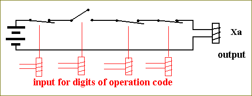
Figure 20. Circuit for recognizing the ADD-operation. The values of the digits of the code, loaded in the Instruction-register, are inputs for a Recognizer-circuit. Here the Recognizer for 0100.
The Add-Recognizer circuit, the carry-circuit (Fc) and the sum-circuit (Fs) together form the complete ADD-circuit for one-digit addition. Whether, in diagrams, we draw Fs at the top, or Fc (at the top), is of course unimportant (in the diagram below -- fig 20) we drawed Fs at the top).
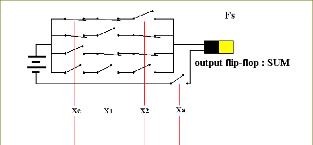
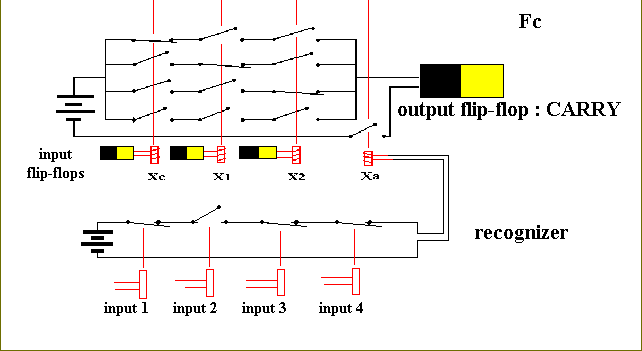
Figure 21. Complete ADD-circuit, for one-digit addition
Let us explain the operation of this (complex) circuit in more detail.
The circuit should add two binary digits, return their sum and carry. So let us add the two binary digits 1, i.e. we want to compute 1 + 1.
We assume that the flip-flop Xc stores a 0, that is, we assume that there is no carry from a previous calculation : Xc = 0. In the flip-flop X1 is stored a 1, and in the flip-flop X2 also a 1 is stored, so X1 = 1, and X2 = 1. And because we also assume that the Instruction-register currently contains the code 0100 for the ADD-OPERATION, implying that input1, input2, input3, and input4 of the Recognizer Circuit have values of respectively 0, 1, 0, 0, the variable Xa is set to 1, the circuit is activated : Xa = 1.
So the input (configuration) is : 0 1 1 1.
In the diagram of Figure 21 we must now imagine that the Xa-switches are closed, because they are pulled down, according to Xa being 1.
Along the line of Xc (see again the diagram) the switches are NOT pulled down (because Xc = 0).
Along the line of X1 the switches are pulled down (because X1 =1).
Along the line of X2 the switches are pulled down (because X2 =1).
In the circuit for Fs, the SUM-circuit, this results in the following switch-configuration :
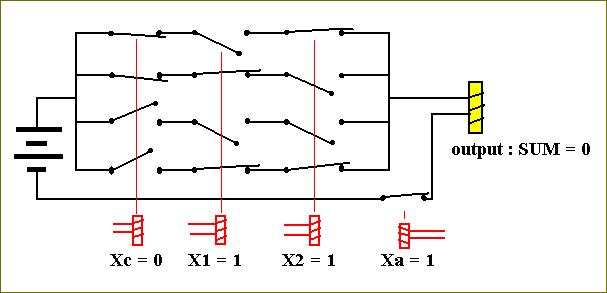
It is clear that with this configuration no current can flow, so the output will be 0 and will be stored in the output flip-flop (not shown in the above diagram, but shown in Figure 21). So the circuit has indeed correctly calculated the binary sum of 1 and 1.
Now we look to the other circuit of the adder, the carry-circuit, that computes the function Fc, the carry (value). Here the same values for Xc, X1, X2 and Xa apply. These values were respectively : 0, 1, 1, 1.
So the Xa-switches are closed, because Xa = 1.
The Xc-switches are NOT pulled down (because Xc = 0).
The X1-switches are pulled down (because X1 = 1).
The X2-switches are pulled down (because X2 = 1).
This results in the following switch-configuration for the circuit that computes the carry (i.e. computes the function Fc) :
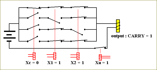
We can see that the current can pass, because (at least) one row consists of closed switches. So the output of the carry-circuit is 1, which means a carry of 1. And indeed this is correctly computed, because the binary sum of 1 and 1 equals 0 and has carry 1. In a more-then-one-digit addition this carry-value will be transported to the next column (of digits to be added) to the left. As another test we could try the one-digit addition of 0 and 1. This results in the sum being equal to 1, and the carry-value being equal to 0.
We now have fully expounded a complete circuit (with relays as its elements) for one-digit addition. If registers with many digits are to be added (i.e. subjected to the operation of addition), then many copies of the single-column adder together will do the task. We can imagine how, for example, a 4-digit addition device schematically looks like when we wire 4 copies of the device of Figure 17 together :
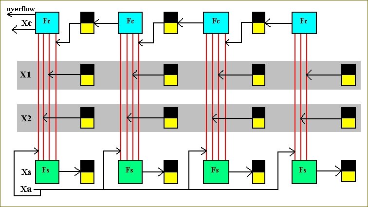
Figure 22. A device for adding the content of two 4-bit registers.
This concludes our exposition of basic computer-circuits, built with relays. The logical design of modern computers (which use transistors instead of relays) is not necessarily the same as that here expounded. The sole purpose was to present some fundamental concepts, that clarify how to " make electricity think ". Only these fundamentals are necessary for an ontological evaluation of Artificial Life creations, for which this Essay forms a preparation.
In order to understand more of the material (i.e. the matter, especially matter as substrate) of modern computers, and to experience some more circuitry, we will treat of transistors. Transistors are electronic switches, that are minute, energy-economic and fast. They form the ' Silicon ' of the modern machines. Thousands of them are integrated in such machines.
Transistors
Because with transistors we have very small and fast switches, we can integrate them into assemblies consisting of a huge number of them : integrated circuits. Such an integrated circuit will accordingly have small dimensions, thus making the connections very short, which again reduce the time needed for the electrical current to flow across such an integrated circuit, so they become fast, i.e. even very complicated tasks can be executed in a very short time. Let us explain how transistors work.
Electrical Conduction
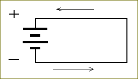
Materials consist of atoms. Each atom has a nucleus that is surrounded by electrons. These electrons are distributed over so called concentric shells. Each shell can hold a certain maximum number of electrons. Most properties of materials, including electric conductivity, are largely determined by the (number of) electrons in the outermost shell [For atomic structure , see The Essay on the Chemical Bond ]. So in metals, with only one electron in the outermost shell of each of their atoms, it appears that those electrons are not tightly held to their own atoms. They can move freely through the material. So if we make a wire-loop of such material, for example copper, and insert a battery, then an electrical current will develop, because the battery tries (and in this case successfully) to send electrons from its negative pole (symbolized by the shorter outer bar in the symbol for a battery) and to collect them at its other (positive) end (this end is symbolized by the longer bar) :
Some other materials are semiconductors for instance Silicon and Germanium. The arrangement of the atoms of these materials is such that each atom is surrounded by four neighbor atoms. Each atom has four electrons in its outermost shell, and such materials are not necessarily good electrical conductors. Each atom shares these four electrons with its four neighbors. So each atom is surrounded in its outermost shell by these four electrons and one donated (i.e. held commonly) by each of its four neighbors. This form is very stable : The eight electrons are held tightly between the atom cores. Hence no electrons are available for conduction :
![]()
Figure 23. A battery applied across a Silicon crystal. The black dots symbolize the Silicon atoms, and the red spots symbolize electrons of their outermost shells. Very little electric current will flow.
But, it turns out that we can engineer the conductivity properties of such a semiconductor. In a Silicon crystal there are no electrons available that can freely move (and will produce a current when an electromotive force -- by means of a battery -- is applied). In other words, we have no carriers . However we could supply such carriers as follows : When, in a Silicon crystal, we replace one Silicon atom by an atom of Phosphorus, then this Phosphorus atom will neatly fit into the crystal-lattice. Phosphorus atoms have five electrons in their outer shell. They share four of them with their Silicon neighbors, but the fifth electron donated by Phosphorus has no stable home and it can be moved by an electromotive force. When we insert, say, several Phosphorus atoms per million Silicon atoms, then their are enough conductor electrons to support an electrical current. Such a Silicon crystal, provided with such ' impurities ', are called n-type doped material, because negative , electrons, are added to achieve conductivity.
![]()
Figure 24. A battery applied across an n-type doped Silicon crystal. The extra electrons can support a current.
There are other ways to make crystalline Silicon into a conductor. One such way is to replace some Silicon atoms by Boron atoms. Boron atoms have only three electrons in their outer shell. So when such a Boron atom replaces a Silicon atom, it will try to fit in like the other Silicon atoms among each other. But to do so it misses one electron. We can imagine this missing electron as a hole. These holes can shift from atom to atom causing a net movement of charge. This type of crystal, where the carriers are holes, are called p-type doped material.
![]()
Figure 25. A battery applied across a p-type doped Silicon crystal. The holes can migrate from atom to atom (which is the case when an electron from some neighboring atom ' jumps ' into that hole, and leaving behind another hole created by this jumping away) and can accordingly support an electical current.
Thus p-type doped Silicon can be thought of as material with occasional holes here and there where electrons can fit, and n-type doped Silicon is just the opposite, with extra electrons scattered around.
If (material of) the two types are juxtaposed, some of the extra electrons on the n-side will fall across the boundary into holes in the p-side. This means that in the boundary region many carriers (holes on one side of the boundary and free electrons on the other) have disappeared, causing the boundary region poorly-conductive. This can be seen when we apply a battery across the material in the way indicated by Figure 26. In fact the battery will enhance this inconductivity because it fills up the holes above (in the p-type part) and sucks the extra electrons away from below (the n-type part), resulting in the absence of carriers:
![]()
Figure 26. A battery applied across juxtaposed n-type doped Silicon and p-type doped Silicon. In the direction imposed by the battery only little current can flow through the material.
However, if the battery is reversed, a great change occurs. Now the battery supplies more free electrons into the lower part and sucks electrons away from the upper part, which means that the carriers are constantly being replenished, resulting in good conductivity of the device :
![]()
Figure 27. The same as Figure 26, but now with the battery reversed. A good conductivity is the result. A strong electric current is flowing through the device.
What we in fact have constructed is a one-way valve. It allows current only in one direction, the n-p direction. Such a device is called a diode. But what we most need is a device that lets one circuit control another circuit, just like the relays we treated of earlier. Most important is that a low powered circuit can control (i.e. switch on and off) a high(er) powered circuit. So what we need is a kind of switch, analogous to the relay.
Construction of the Transistor
The next step is building a device consisting of three consecuted layers of doped Silicon : A top layer of n-type doped Silicon, called the Collector, a middle layer of p-type doped silicon, called the Base, and a bottom layer of n-type doped Silicon, called the Emitter. When we apply a battery across the emitter-base junction a current will flow, because a current will more easily flow across a n-p junction than it will across a p-n junction :
![]()
Figure 28. A small battery applied across the emitter-base junction of a three layered device, made of doped Silicon. A current will flow from the battery through the emitter-base junction, and then back to the (other end of the) battery.
Next let us switch off this ' base current ' and apply a large battery across the whole device :
![]()
Figure 29. A large battery applied across a three layered device of doped Silicon of which the base current (from a small battery) is switched off.
Electrons cannot flow from the small battery to the emitter-base junction and back to that battery, because this loop is switched off (it is interrupted by the open switch). So now the current from the large battery will try to flow through the emitter-base junction, but then it encounters a p-n junction, and such a junction will not support current in that direction. Thus there will not flow any current from the large battery through the device and back to that battery, and other possibilities are not present.
But if the small battery is reconnected (by closing the switch), current will flow from the small battery through the emitter-base junction of the device and back into the small battery. So carriers move through the base, and some of these carriers will diffuse across the base-collector junction and consequently will allow it to pass current. Furthermore, in a well designed device (by means of placing some resistors at appropriate places) MOST of the carriers flowing from the emitter will drift into the collector so a rather SUBSTANTIAL current will flow. See Figure 30.
![]()
Figure 30. The same as figure 29, but now with the base current on.
So what we have is the following :
A low powered circuit controlls a high powered circuit : If and when the low powered circuit is ON, current will flow in the high powered circuit, i.e. the high powered circuit is turned ON. If an when the low powered circuit is OFF, there will be no current in the high powered circuit, i.e. the high powered circuit is turned OFF. So the desired switch, built from a doped semiconductor has been constructed. Such a three-layer device is called a transistor. This transistor can be switched ON and OFF by a base current input, and in so doing it can switch ON and OFF a certain circuit.
We now will show how transistors can be used to build computer circuits.
Construction of Transistor-based Computer Circuits
We shall now build a circuit, based on transistor technology, that can compute a useful function :
![]()
Figure 31. A transistor-based computer circuit.
The circuit consists of two diodes (n-p junctions), a transistor (n-p-n junction), a few resistors, a small battery Bs and a large battery BL, an output device, that we can imagine being a light bulb, and two input circuits.
Both input circuits, X and Y, should be interpreted as follows : If and when X = 1, the corresponding input circuit has a non-zero voltage and accordingly acts like a battery :
If and when X = 0, the corresponding input circuit has zero voltage and will act as if it is a simple wire.
Precisely the same applies to input Y.
The analysis that follows will examine the behavior of the circuit assuming each input can have these two behaviors.
Let us begin by assuming that both inputs are zero, i.e. X = 0 and Y = 0 :
![]()
Figure 32. The computer circuit of Figure 31, for X = 0 and Y = 0.
We want to investigate what the output F will be, 1 or 0 (lightbulb on or off).
The electrons from the small battery (Bs) will try to leave the negative end (corresponding to the lowest short bar) and collect again at the positive end of the battery. In so doing they go to the left, flow through both input circuits, through both diodes (i.e. the easy way from n to p) and then, via a small resistor, back to the (small) battery. Because electrical current always takes the easiest route, it will not, after leaving the negative end of the battery, go to the right, go across the emitter-base junction of the transistor and then back to the (small) battery, because this route contains two resistors. This implies that there is no current flowing through the emitter-base junction of the transistor causing the transistor to be OFF. We symbolize this by not drawing the transistor completely, thus emphasizing its non-conductive status.
Next we watch the behavior of the current from the large battery (BL). It will also attempt to force electrons out of its lower wire and collect them at the top. So the current will go to the right, and because the transistor is shut down, it will pass through the output device (the light bulb) and the lamp will be ON, i.e. the output, F, is 1.
So our first result is :
Let us now examine the behavior of the circuit for X = 1 and Y = 0 :
![]()
Figure 33. The computer circuit of Figure 31, for X = 1 and Y = 0.
In this case the X input will act like a battery. It will push electrons down its lower wire, but then this current encounters the current from the small battery, Bs, coming from the opposite direction. When we assume that the strenght of the ' battery ' of the X input (the same applies to the Y input when it is on) is the same as that of the small battery, Bs, then it is clear that the two currents, coming from opposite directions, will cancel each other, and this means there will be no current in the upper left region of the circuit. The upper diode consequently does not have any current passing through it, and is drawn as interrupted. But, because Y = 0, the current from the small battery, Bs, is still allowed to pass through the circuit of the Y input and so follow its course through the lower diode and back again to the (small) battery. This is still an easy path, compared with the other alternative path : Going (after leaving the lower end of the small battery, Bs) to the right, then through the emitter-base junction of the transistor and back into the (small) battery, because this path contains two resistors. So the transistor will remain OFF, and the current from the large battery, BL, must go through the output device (the light bulb) and the lamp will remain ON, i.e. F = 1.
So our second result is :
A similar situation occurs when X = 0 and Y = 1 :
![]()
Figure 34. The computer circuit of Figure 31, for X = 0 and Y = 1.
Here the easiest path for the current from the small battery, Bs, is through the X input circuit, and then via the diode back to the battery again. So no current is flowing through the emitter-base junction of the transistor, resulting in it to be OFF, implying F = 1.
So our third result is :
Let us finally examine the last possible input-configuration, namely X = 1 and Y = 1 :
![]()
Figure 35. The computer circuit of Figure 31, for X = 1 and Y = 1.
In this case the current from the small battery cannot flow to the left, because it is now totally blocked by the two currents from the inputs X and Y (these inputs now both act as if they were batteries). This implies that the current, coming from the lower end of the small battery, Bs, must go to the right and will consequently flow through the emitter-base junction of the transistor causing it to be ON. The transistor can accordingly be drawn just like a line. Therefore the current, coming from the large battery, BL, will take its easiest path through the transistor and then flow back to the positive end of the large battery. It will not flow through the output-device, because this device is in fact a resistor, and therefore this path (through the output-device) will not be the easiest path to follow. So the lamp will go OFF, i.e. F = 0.
So our fourth and final result is :
The analysis of the behavior of the circuit is now complete, and can be summarized in the following function-table :
X    Y         F
----------------
0    0         1
0    1         1
1    0         1
1    1         0
----------------
This circuit is called a NOR circuit, and is symbolized as follows :
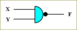
Figure 36. Symbol for the NOR circuit.
It is the only building-block needed for constructing all the circuits that were treated of above, using relays :
So the NOT circuit can be built from a NOR circuit by omitting the Y input circuit :
![]()
Figure 37. The Transistor-based circuit for computing the NOT-function.
We can symbolize this transistor-based NOT circuit as follows :
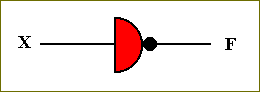
Figure 38. Symbol for the NOT circuit.
The function-table for the NOT-function is :
X      F
--------
0      1
1      0
--------
We can construct the AND (transistor-based) circuit by combining the NOR and the NOT circuits, i.e. by negating the output of the NOR circuit, NOT[NOR] = AND, because, when we flip each output of the NOR-function, we get the AND-function :
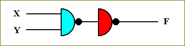
Figure 39. Symbol for the AND circuit.
The function-table for the AND-function is accordingly :
X    Y         F
----------------
0    0         0
0    1         0
1    0         0
1    1         1
----------------
We can also construct the transistor-based circuit for computing the OR-function. This we do by computing the NOR-function of the negated X and the negated Y, NOR[ NOT[X] NOT[Y] ] :
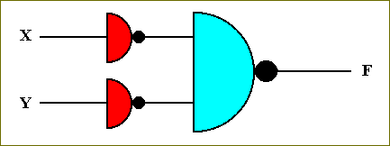
Figure 40. Symbol for the OR circuit.
This circuit, for computing the OR-function can be determined by showing how to generate the table for the OR-function :
X    Y         F
----------------
0    0         0
0    1         1
1    0         1
1    1         1
----------------
When we compare the output series of this function with that of the NOR-function, we can imagine this output series (of the OR-function) as being the output of some NOR-function. Indeed if we negate X and negate Y, then we get the following values for these negated variables (X and Y) :
NOT[X]  NOT[Y]         F
--------------------------
1       1              0
1       0              1
0       1              1
0       0              1
--------------------------
This is clearly the function NOR[ NOT[X] NOT[Y] ]. And now it is easy to construct the circuit. We take the symbols for NOT[X] and NOT[Y], and make them the elements of a NOR-function (See Figure 40).
The determination of this circuit can be summarized in the following table where the steps are shown together :
X    Y      NOT[X]  NOT[Y]         F (= OR[XY] = NOR[ NOT[X] NOT[Y] ])
------------------------------------
0    0      1       1              0
0    1      1       0              1
1    0      0       1              1
1    1      0       0              1
------------------------------------
Of course we can have a NOR-function with 3 or more variables, for example NOR[XYZ] :
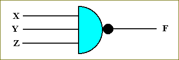
Figure 41. A NOR circuit for three variables X, Y, Z.
The corresponding function-table is :
X    Y     Z            F
-------------------------
0    0     0            1
0    0     1            1
0    1     0            1
0    1     1            1
1    0     0            1
1    0     1            1
1    1     0            1
1    1     1            0
-------------------------
The Transistor-based One-digit Addition Circuit
With our knowledge of transistor-based switches and circuits, we can again construct the circuit that can execute one-digit (binary) addition, but now a transistor-based circuit. One-digit addition means that we confine ourselves to the addition (of two digits) within one column only. We determine the Sum and the Carry. For example, the binary digits 1 and 1 will be added :
1
1
--- +
0 (sum digit)
carry = 1 (carry digit)
So we need the corresponding functions Fs and Fc, described earlier, defining the sum digit and the carry digit respectively.
Let us start with the function Fs. We want to build (i.e. draw) a transistor-based circuit (using the above symbols) that can compute the function Fs. The table (which was already given earlier), that explicitly defines the Sum (digit), is as follows (Because we assume that the coresponding circuit is turned on, i.e. Xa = 1, we only have to consider the three variables Xc, X1 and X2) :
Xc    X1    X2          Fs
--------------------------
0     0     0           0
0     0     1           1
0     1     0           1
0     1     1           0
1     0     0           1
1     0     1           0
1     1     0           0
1     1     1           1
--------------------------
Where Xc is the carry of a previous calculation, X1 the upper digit in the column (formed by the two digits to be added), that should be added to X2, the lower digit in the column.
Xc    X1    X2          Fs1          Fs2          Fs3          Fs4
------------------------------------------------------------------
0     0     0           0            0            0             0
0     0     1           1            0            0             0
0     1     0           0            1            0             0
0     1     1           0            0            0             0
1     0     0           0            0            1             0
1     0     1           0            0            0             0
1     1     0           0            0            0             0
1     1     1           0            0            0             1
------------------------------------------------------------------
We now want to determine the identity of each of the functions Fs1, Fs2, Fs3, and Fs4, i.e. we try to answer the question as to what functions they are. Are they AND-functions, OR-functions, NOT-functions, NOR-functions, or combinations of these?. We start with Fs1.
Xc    X1    X2
--------------
0     0     0
0     0     1
0     1     0
0     1     1
1     0     0
1     0     1
1     1     0
1     1     1
--------------
The next columns (of the table to be constructed) contain values of elementary functions of respectively Xs, X1 and X2. For example when Xc has the value 1, as it is the case in the last four entries of the first column, then NOT[Xc] has the value 0. So NOT[Xc] negates all the values of Xc written down in the first column :
Xc    X1    X2    NOT[Xc]
-------------------------
0     0     0     1
0     0     1     1
0     1     0     1
0     1     1     1
1     0     0     0
1     0     1     0
1     1     0     0
1     1     1     0
-------------------
The same applies to NOT[X1], and also NOT[X2].
Xc    X1    X2    NOT[Xc]    NOT[X1]    NOT[X2]    NOR[ NOT[Xc] NOT[X1] NOT[X2] ]
---------------------------------------------------------------------------------
0     0     0     1          1          1          0
0     0     1     1          1          0          1
0     1     0     1          0          1          1
0     1     1     1          0          0          1
1     0     0     0          1          1          1
1     0     1     0          1          0          1
1     1     0     0          0          1          1
1     1     1     0          0          0          1
-----------------------------------------------------
But we can also leave the value of one or more variables the same, by not applying any function to them (we could equivalently say that we apply to them the identical function, meaning that the values of the input reappear unchanged in the output). For instance we could apply the NOT-function to Xc and to X1, and apply the identical function to X2. And then we could interpret the values of these functions as inputs of the NOR-function :
Xc    X1    X2    NOT[Xc]    NOT[X1]    X2         NOR[ NOT[Xc] NOT[X1] X2 ]
----------------------------------------------------------------------------
0     0     0     1          1          0          1
0     0     1     1          1          1          0
0     1     0     1          0          0          1
0     1     1     1          0          1          1
1     0     0     0          1          0          1
1     0     1     0          1          1          1
1     1     0     0          0          0          1
1     1     1     0          0          1          1
-----------------------------------------------------
When we add another column that writes the NEGATED values of the NOR-column, then we finally get the following table :
Xc  X1  X2  NOT[Xc]  NOT[X1]  X2   NOR[ NOT[Xc] NOT[X1] X2 ]  NOT[ NOR[ NOT[Xc] NOT[X1] X2 ]]
---------------------------------------------------------------------------------------------
0   0   0   1        1        0    1                          0
0   0   1   1        1        1    0                          1
0   1   0   1        0        0    1                          0
0   1   1   1        0        1    1                          0
1   0   0   0        1        0    1                          0
1   0   1   0        1        1    1                          0
1   1   0   0        0        0    1                          0
1   1   1   0        0        1    1                          0
---------------------------------------------------------------
When we look at the values of the last column of this table, then we see in fact the values of the function Fs1, i.e. the first function from the set of four functions (Fs1, Fs2, Fs3, Fs4) obtained by analysing the function Fs. It is now clear that when we want to identify a given function -- given the outputs -- we can, from this given output work backwards to construct a table like the one above, and in this way identify the function, i.e. analyse it in terms of elementary functions.
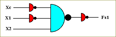
Figure 42. The circuit that computes the function Fs1.
Now we can, using this method, identify the remaining functions Fs2, Fs3 and Fs4, and determine the transistor-based circuits that computes them (and we know that an OR combination of these four functions is equivalent to the function Fs).
Identification of the function Fs2 :
Xc  X1  X2  NOT[Xc]  X1  NOT[X2]   NOR[ NOT[Xc] X1 NOT[X2] ]  NOT[ NOR[ NOT[Xc] X1 NOT[X2] ]]
                                                              = Fs2
---------------------------------------------------------------------------------------------
0   0   0   1        0   1         1                          0
0   0   1   1        0   0         1                          0
0   1   0   1        1   1         0                          1
0   1   1   1        1   0         1                          0
1   0   0   0        0   1         1                          0
1   0   1   0        0   0         1                          0
1   1   0   0        1   1         1                          0
1   1   1   0        1   0         1                          0
---------------------------------------------------------------
From this analysis we can determine the circuit that computes the function Fs2 :
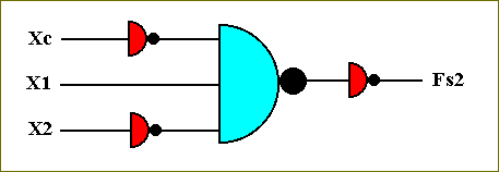
Figure 43. The circuit that computes the function Fs2.
Next we will identify the function Fs3, and determine the associated circuit :
Xc  X1  X2  Xc  NOT[X1]  NOT[X2]  NOR[ Xc NOT[X1] NOT[X2] ]  NOT[ NOR[ Xc NOT[X1] NOT[X2] ]]
                                                             = Fs3
--------------------------------------------------------------------------------------------
0   0   0   0   1        1        1                          0
0   0   1   0   1        0        1                          0
0   1   0   0   0        1        1                          0
0   1   1   0   0        0        1                          0
1   0   0   1   1        1        0                          1
1   0   1   1   1        0        1                          0
1   1   0   1   0        1        1                          0
1   1   1   1   0        0        1                          0
--------------------------------------------------------------
The circuit that computes this function is accordingly :
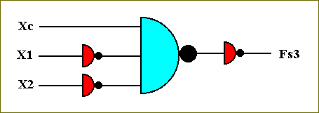
Figure 44. The circuit that computes the function Fs3.
Next we identify the function Fs4 :
Xc  X1  X2     NOR[Xc X1 X2]     NOT[ NOR[Xc X1 X2]]
                                 = Fs4
----------------------------------------------------
0   0   0      1                 0
0   0   1      1                 0
0   1   0      1                 0
0   1   1      1                 0
1   0   0      1                 0
1   0   1      1                 0
1   1   0      1                 0
1   1   1      0                 1
----------------------------------
The associated circuit is accordingly :
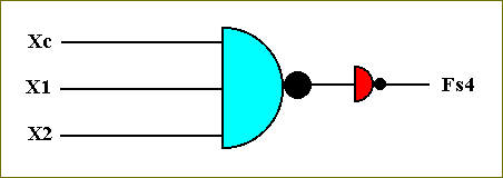
Figure 45. The circuit that computes the function Fs4.
These four circuits must now be connected via the OR-function. This we do (see Figure 40) by negate each of these circuits and then connect them via the NOR circuit formed from them :
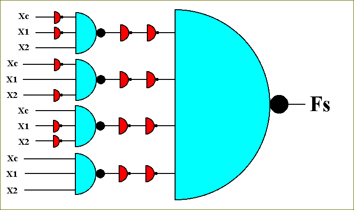
Figure 46. The circuit that computes the function Fs, but still with some redundant circuitry.
But in this circuit we see four times a set of two NOT-circuits placed after each other. From Logic we know however that when something-negated is again negated it will be affirmed : Peter does not not go to school, means he is going to school.
So two NOT's cancel each other. So the circuit for the function Fs becomes :
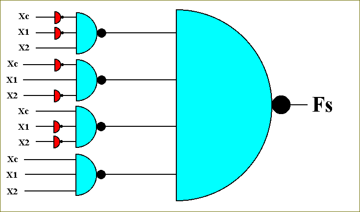
Figure 47. The circuit that computes the function Fs.
For a check, let us fill in Xc = 0, X1 = 0, X2 = 1. According to the function-table of the function Fs the output should be 1.
When we fill in the values of Xc, X1, and X2, into the circuit-diagram, and follow them from left to right, we indeed find that for this set of input-values the output becomes 1 :
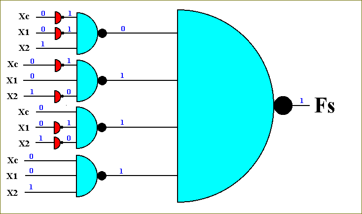
Figure 48. Determination and check of the output of the circuit for Fs, where Xc = 0, X1 = 0, and X2 = 1.
A more convenient way of drawing the circuit-diagram for the function Fs is the following :
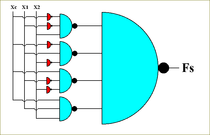
Figure 49. The circuit for the function Fs.
This concludes the construction of the transistor-based circuit for computing the function Fs.
Next we must construct the transistor-based circuit that computes the function Fc.
Remember that the functions Fs (sum-bit) and Fc (carry-bit) together constitute the one-bit ADDING function.
Construction of the circuit for Fc.
Again we assume that the circuit that corresponds to Fc is switched on, i.e. Xa = 1 (So we only have to consider the variables Xc, X1, and X2).
By realizing precisely what -- in binary notation -- calculating the value of the carry, when we add two binary digits together (i.e. a one-column addition) actually is, we can construct the table for this carry-function, Fc :
Xc  X1  X2      Fc
------------------
0   0   0       0
0   0   1       0
0   1   0       0
0   1   1       1
1   0   0       0
1   0   1       1
1   1   0       1
1   1   1       1
-----------------
We can dissect this function into four functions (and they are connected by the OR-function). Those functions are Fc1, Fc2, Fc3, Fc4 :
Xc  X1  X2       Fc1      Fc2      Fc3      Fc4
-----------------------------------------------
0   0   0        0        0        0        0
0   0   1        0        0        0        0
0   1   0        0        0        0        0
0   1   1        1        0        0        0
1   0   0        0        0        0        0
1   0   1        0        1        0        0
1   1   0        0        0        1        0
1   1   1        0        0        0        1
---------------------------------------------
Again we analyse these functions into their elementary components in order to determine the circuit that computes them :
Xc  X1  X2    NOT[Xc]  X1  X2   NOR[ NOT[Xc] X1 X2 ]    NOT[ NOR[ NOT[Xc] X1 X2 ]]
                                                        = Fc1
----------------------------------------------------------------------------------
0   0   0    1         0   0    1                       0
0   0   1    1         0   1    1                       0
0   1   0    1         1   0    1                       0
0   1   1    1         1   1    0                       1
1   0   0    0         0   0    1                       0
1   0   1    0         0   1    1                       0
1   1   0    0         1   0    1                       0
1   1   1    0         1   1    1                       0
---------------------------------------------------------
The transistor-based circuit for computing this function is accordingly :
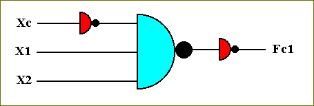
Figure 50. The circuit that computes the function Fc1.
The table for the function Fc2 is :
Xc  X1  X2     Xc  NOT[X1]  X2   NOR[ Xc NOT[X1] X2 ]     NOT[ NOR[ Xc NOT[X1] X2 ]]
                                                          = Fc2
------------------------------------------------------------------------------------
0   0   0      0   1        0    1                        0
0   0   1      0   1        1    1                        0
0   1   0      0   0        0    1                        0
0   1   1      0   0        1    1                        0
1   0   0      1   1        0    1                        0
1   0   1      1   1        1    0                        1
1   1   0      1   0        0    1                        0
1   1   1      1   0        1    1                        0
-----------------------------------------------------------
The transistor-based circuit for computing this function is :
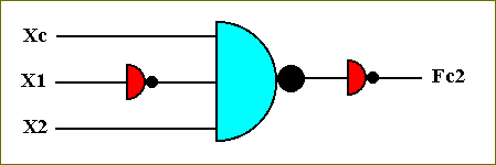
Figure 51. The circuit for computing the function Fc2
The table for the function Fc3 is :
Xc  X1  X2    Xc  X1  NOT[X2]     NOR[ Xc X1 NOT[X2] ]      NOT [ NOR[ Xc X1 NOT[X2] ]]
                                                            = Fc3
---------------------------------------------------------------------------------------
0   0   0     0   0   1           1                         0
0   0   1     0   0   0           1                         0
0   1   0     0   1   1           1                         0
0   1   1     0   1   0           1                         0
1   0   0     1   0   1           1                         0
1   0   1     1   0   0           1                         0
1   1   0     1   1   1           0                         1
1   1   1     1   1   0           1                         0
-------------------------------------------------------------
The transistor-based circuit for computing this function is accordingly :
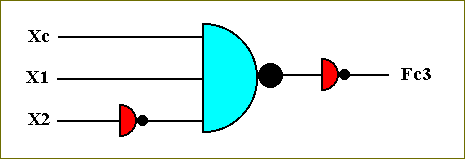
Figure 52. The circuit for computing the function Fc3.
The table for the function Fc4 is :
Xc  X1  X2       NOR[ Xc X1 X2 ]       NOT[ NOR[ Xc X1 X2 ]]
                                       = Fc4
------------------------------------------------------------
0   0   0        1                     0
0   0   1        1                     0
0   1   0        1                     0
0   1   1        1                     0
1   0   0        1                     0
1   0   1        1                     0
1   1   0        1                     0
1   1   1        0                     1
----------------------------------------
The transistor-based circuit for computing this function is accordingly :
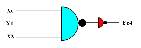
Figure 53. The circuit for computing the function Fc4.
In order to get the complete circuit for the function Fc we must combine these four circuits by means of the OR-function (See Figure 40). This we do by negating the output of each of the functions (Fc1, Fc2, Fc3, Fc4) and then make them the elements of a NOR circuit :
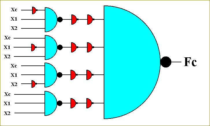
Figure 54. The circuit for the function Fc. There is still some redundancy in the circuit.
Again we see four sets of two negations (NOT-circuits) placed after each other. These will cancel :
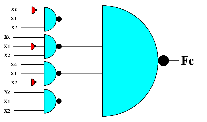
Figure 55. The circuit for the function Fc. The redundancy is removed.
This circuit (for the function Fc ) is more conveniently drawn as follows :
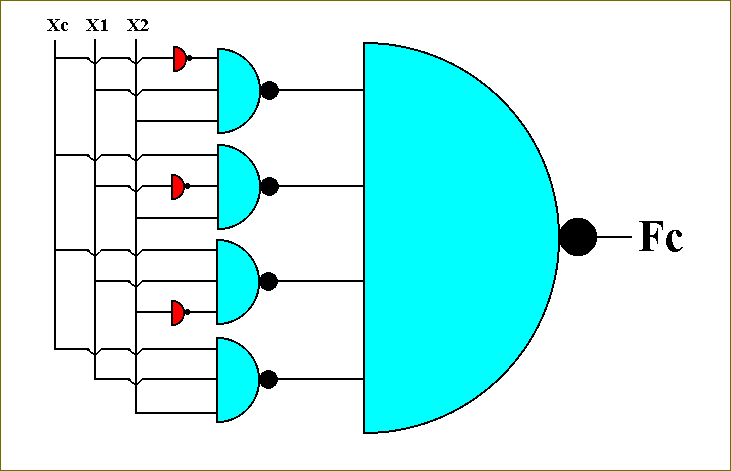
Figure 56. The circuit for computing the function Fc
So this finally is the transistor-based circuit for computing the function Fc.
The circuits for Fs and for Fc together form the circuit that can execute one-digit binary addition. The circuits for Fs and Fc have a common input : the values of the three variables Xc, X1, and X2. They are fed into both circuits simultaneously and cause the Fs-circuit to compute the sum-digit, and the Fc-circuit to compute the carry-digit :
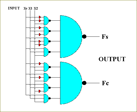
Figure 57. The transistor-based circuit for executing one-digit binary addition.
So we now have the complete transistor-based circuit for one-digit binary addition. An input triple (values for Xc, X1, and X2) causes the circuit to compute the sum X1 + X2 and the new carry-value. This new carry-value, Fc, will, in the next calculation -- in case of a more-than-one digit addition -- be attributed to the variable Xc, representing in this next calculation the carry generated by the previous calculation.
When we compare this circuit with the corresponding relay-based circuit, then we see that the NOT-circuits, pictured as

correspond to the relay-based NOT-switches.
With the example of a transistor-based circuit that can compute one-digit binary addition, we conclude this section on Transistors.
Transistors and their derivatives provide the millions of switches needed in modern computing machinery. Together they form integrated circuits in such machines.
Basic Design of the Digital Computer
We have learned how to build circuits for computing functions. Now we must find out how all these circuits can work together to constitute a computer. Recall, figures 20 and 21. There we drew a circuit called a recognizer. If and when such a circuit outputs a 1, a certain other circuit -- a computational circuit -- will be switched on. Each computational circuit is in this way associated with a recognizer circuit :
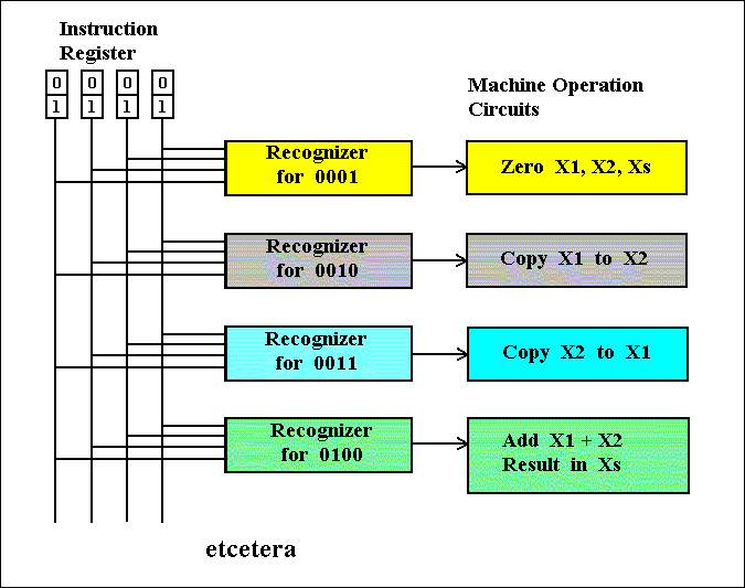
Figure 58. The Instruction Register, Recognizer-circuits and Machine Operation Circuits. Depending on the code in the Instruction Register, a certain Machine Operation Circuit will be switched on.
The Instruction Register, the Recognizer-circuits and the Machine Operation Circuits form a part of the CENTRAL PROCESSING UNIT (CPU) of the computer. Besides this CPU the computer contains a MEMORY BOARD. This board consists of a large amount of storage-circuits. The CPU fetches information (instructions and data) from the MEMORY, executes the instructions on the data, and returns the result to the MEMORY.
The instructions are binary codes and they are sequentially brought into the Instruction Register, IR, of the CPU, and -- sequentially -- executed. A so called Instruction Pointer Register, IP, shows the particular memory address where to find and fetch the particular instruction. When that instruction is fetched and brought (as a copy) into the Instruction Register, the Instruction Pointer Register will indicate the next memory address for fetching the next instruction, as soon as the previous instruction has been carried out. This executing of an instruction is carried out by the appropriate computational circuit -- switched on by the corresponding recognizer circuit. The result of the execution will be placed in another register of the CPU, the Computation Register, AX. The instructions correspond to primitive operations like copying the content of a memeory location into the Computation Register AX of the CPU, or adding the content of a memory location to the content of the Computational Register AX, and leave the result in AX.
Data and instructions normally reside in memory in the form of binary sequences, like 0100, 1100, etc. When a programmer wants the computer to compute something, she must anatomize the desired computation into a set of primitive operations, for which the CPU contains the corresponding circuits. This set of primitive operations to be executed corresponds directly with the set of instructions, instructions which must sequentially loaded into the Instruction Register of the CPU. Because programming with binary sequences is very inconvenient, the programmer uses a (suggestive) name for each instruction. The set of those names and their syntax that must be used to write a computer program is called Assembly Language. The programmer types those names in the required order and those names are immediately translated into machine code, i.e. sequences of 0's and 1's. In our exposition we will not use the binary form of the instructions. Instead of that we represent those binary codes by the Assembly Language expressions placed between asterisks (**). So when the instruction for, say, copying the content of memory location M1 into the Computational Register AX of the CPU, is, say, 0011, then we denote this by :
So COPY AX,M1 is the instruction, while *COPY AX,M1* is its binary code. Also the data are present in the memory in the form of binary sequences : (for example) *7* means 0111, the binary expression for 7.
The CPU-Memory configuration of a simple type of digital computer could look like this (See also BIERMANN, 1990, Great Ideas in Computer Science , pp. 252):
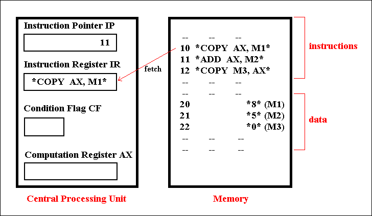
Figure 59. Outline of the CPU-Memory configuration of a simple type of digital computer.
The index for the memory location of the instruction *COPY AX, M1* is 10 (of course also coded in binary), and so this instruction will be placed in the Instruction Register IR of the CPU. The Instruction Pointer will now change to the next index, 11. The instruction will be decoded by the mechanism shown in figure 58, which means that the appropriate circuit is turned on. That circuit now executes the instruction COPY AX, M1 and this means that the content of memory location M1 will be copied into the Computation Register AX of the CPU. Now the next instruction, *ADD AX, M2*, is fetched and placed in the Instruction Register, replacing the previous instruction. The Instruction Pointer now sets itself to 12. Decoding and executing the instruction ADD AX, M2 means that the content of memory location M2 is added to the content of AX, and the result (content of M2 + content of AX) remains in AX. Now the next instruction is fetched and placed in the Instruction Register, while the Instruction Pointer goes to 13. This instruction *COPY M3, AX*, will be decoded and executed, resulting in placing the content of AX in memory location M3. Summarizing this all, say we want to add two numbers 8 and 5. The number 8 is present in memory location M1, while the number 5 is in memeory location M2. The result of the addition, 13 (8 + 5), is placed (as *13*) in memory location M3. The Assembly Language program for executing this task was :
Besides the ADD and COPY instructions we will find (circuits for) still other instructions, like MUL (multiply), for example MUL AX, M1, or SUB (subtract), DIV (divide) etc. Other important instructions are of a conditional type. So the instruction CMP that compares two numbers. The result of this comparison will be placed in the Condition Flag, CF. Depending on the outcome of such a comparison either the next index for the memory location will be placed in the Instruction Pointer, resulting in loading the next instruction of the sequence in the Instruction Register, or the Instruction Pointer will jump (i.e. executing a jump-instruction ordered by the program) to another non-consecutive index, causing the machine to jump to an instruction that is not next in the memory sequence. So we could have for instance the instruction CMP AX, M1. This means the following :
If the content of AX is smaller than the content of M1, then the value of the Condition Flag becomes B (CF = B) else the value of the Condition Flag becomes NB (CF = NB). Associated with this condition are two jump-instructions, JNB (jump if not below) and JB (jump if below). JB will be executed if the content of AX is indeed smaller than the content of M1, which causes CF = B. Such a jump-instruction could then be : JB Lab1, which means : Go to the instruction with label lab1 (if CF = B). If the content of AX is not smaller than the content of M1, then CF = NB, and consequently a JNB (jump if not below) instruction will be executed, for example the instruction JNB Lab2, which means : Go to the instruction with label Lab2 (if CF = NB).
Besides these conditional jumps there are also just jumps to be executed. It concerns the instruction JMP (jump), for example JMP Lab3, which means : Go to the instruction with label Lab3.
Thus after such a jump the machine starts to follow (i.e. fetch, decode and execute) a new sequence (in memory) of instructions, or, the same sequence all over again.
We already gave an Assembly Language program for adding numbers. Another example of such a program could be one that computes the absolute value of a given number, i.e. it outputs that same number if it is positive, and outputs its negative if it is negative [ The number to be manipulated is assumed to reside in memory location M1. To output the result -- print it as program output on screen or printer -- is taken care of by the instruction OUT AX. The sign := means gets the value of. ] :
PROGRAM NUMERICAL EXAMPLE (M1 contains the number -5 )If the number in M1 was 5, then we get :
------------------------------------------------------------------------------------------- COPY AX, M1 AX := -5
SUB AX, M1 -5 - (-5) = 0 (i.e. AX := 0)
CMP AX, M1 0 is not below -5, CF := NB, therefore the JB instruction is skipped
JB NEXT If AX is below M1 then go to the instruction with label NEXT
SUB AX, M1 0 - (-5) = 5 (i.e. AX := 5)
COPY M1, AX M1 := 5
NEXT COPY AX, M1 AX := 5
OUT AX print 5
-------------------------------------------------------------------------------------------
AX := 5
5 - 5 = 0 (i.e. AX := 0)
0 is below 5, CF := B, thus the instruction JB (jump if below) must be followed, so the machine must go to the instruction with the label NEXT.
AX := 5
print 5
A processor of a computer contains a number of circuits, among them a set of computational circuits. Depending on, and corresponding with, this set, the processor supports a fixed series of different types of instructions. The programmer (programming in Assembly Language) must select a subset from these available (basic) instructions to compose his computer program. He first thinks about a verbal solution to the problem he wants the computer to solve, the algorithm. Then he tries to translate this algorithm into a sequence of the available basic instructions supported by the processor, i.e. he tries to translate his algorithm into Assembly Language. He accordingly obtains a computer program that can be implemented on the computer (with that particular type of processor), i.e. the Assembly program lines are typed in and directly translated into the corresponding binary codes. These codes will now reside in memory, and can sequentially be brought into the Instruction Register of that processor (CPU).
Even in Assembly Language it is not easy programming because every task must be anatomized into the basic instructions, i.e. the task must be expressed in terms of these elementary instructions like COPY AX, M2. In order to be able to program a computer more conveniently, so called higher programming languages have been created, like for instance the programming language PASCAL. Within this language we can write on a higher level than the level of elementary machine instructions. Along with such a higher language one has developed translators, programs that translate lines of a program written in a higher programming language into basic machine code. The existence and use of such higher programming languages and their associated translators, are not important for our (philosophical) purpose. For investigating the ontological status of a running digital computer it is sufficient to consider the program in machine code (or, as one wishes, in Assembly Language) and contemplate its execution. Each Assembly Language instruction, like ADD AX, M5, COPY AX, M1, etc. corresponds to a certain electrical circuit. These circuits, together with the storage circuits, constitute the interacting elements of the computer when it is interpreted as a dynamical system.
Ontological Interpretation of the Digital Computer
In Part One we discussed the UNIVERSAL TURING MACHINE.
As such this " machine " is not yet a machine, not yet a -- physical -- computer, but just the BARE CONCEPT of a digital computing machine.
In Part Two we have PHYSICALLY EMBODIED this concept by means of the design of electrical circuits, that can actually be constructed from real materials like copper and doped semi-conductor materials.
Only if and when we have actually constructed such a machine by means of those circuits, we have a physical digital computer.
Such a physical computer can be interpreted as a COMPLEX DYNAMICAL SYSTEM. Its interacting elements are its elementary circuits :
A circuit A can receive input from (the output of) circuit B. Circuit B can be either a storage-circuit, or a computational-circuit. The output of this circuit is input for circuit A and could modify its output. This output could itself become the input for circuit A, i.e. for itself, or for another circuit, say, C, or it could be the input for circuit B. So the circuits are interacting with each other, like people in a society, and will give rise to an overall output of the computing machine. When complex interactions take place in such a machine, emergent behavior is to be expected. But all this remains a bottom-up process. These emergent behaviors can play a role in Artificial Life research, but the question whether these behaviors are in some cases ' alive ' or not, is in fact irrelevant for the assessment of the ontological status of those behaviors. The machine can behave in complex ways that we decide to call living. The basic elements of such an artificial life system are the circuits of the physical computer, that is, (only) those circuits that participate directly in the relevant emergent behaviors (i.e. are directly -- be it all the way from the bottom -- responsible for generating them). So computer-based artificial life is a physical process, a physical dynamical system, but its elements are not (macro-) molecules, but (elementary) circuits. Ultimately however the elements are atoms and free electrons.

Go to the HOMEPAGE of this site, so that you can navigate through it, and find my e-mail address.